

A joint Tesla–SpaceX semiconductor venture promises to reshape AI, robotics, and space computing. But can it actually be built?
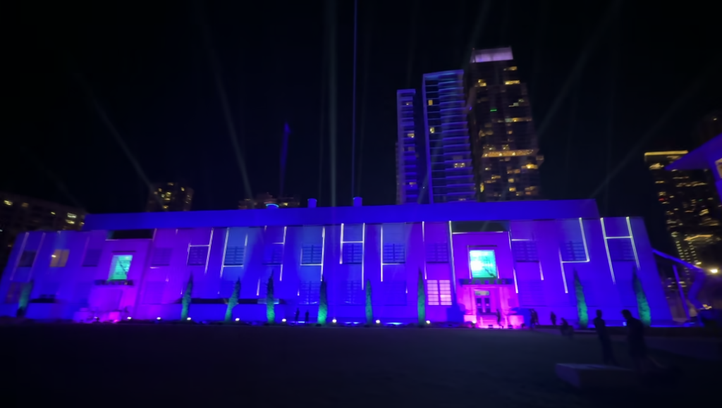
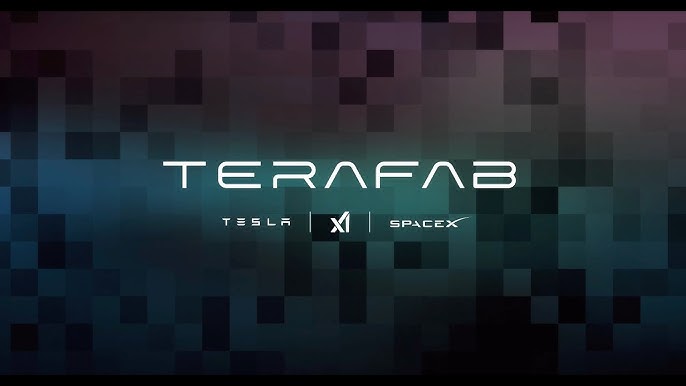
On the night of March 21, 2026, Elon Musk walked onto a stage inside the defunct Seaholm Power Plant in downtown Austin, Texas — a fitting venue, given that he was about to announce something that would require an almost incomprehensible amount of power to realize. Under dramatic lighting, before a crowd of engineers, investors, and journalists, he unveiled Terafab: a joint venture between Tesla, SpaceX, and xAI that he described as “the most epic chip-building exercise in history, by far.”
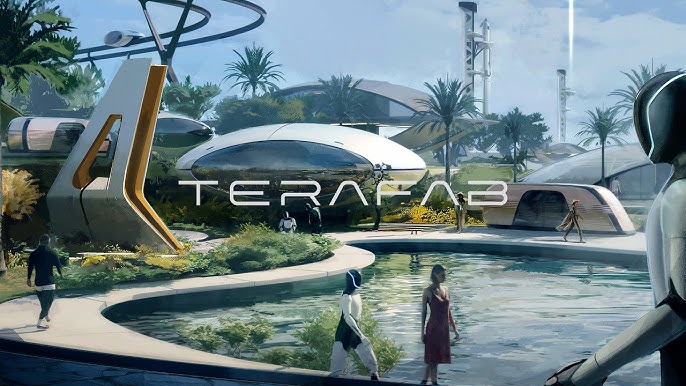
The goal, he said, was to produce 1 terawatt — 1 trillion watts — of computing power per year, most of it deployed not on Earth, but in space. The facility would be built near Tesla’s Gigafactory in Austin, would target 2-nanometer semiconductor process technology, and would consolidate every stage of chip production — design, lithography, fabrication, memory, advanced packaging, and testing — under a single roof. It would, if Musk’s projections hold, produce between 100 and 200 billion custom AI and memory chips annually.
“We either build the Terafab or we don’t have the chips, and we need the chips, so we build the Terafab,” Musk told the crowd.
The reaction from the tech and semiconductor industries was immediate, and split almost perfectly down the middle. Tesla enthusiasts and AI bulls saw a visionary move — a vertical integration play that could give Musk’s empire an unassailable edge in the AI arms race. Semiconductor veterans and skeptical analysts saw something else entirely: a man with no chip manufacturing experience promising to do in a few years what TSMC spent decades and hundreds of billions of dollars building.
Both reactions are understandable. Terafab is, depending on your perspective, either the most important industrial announcement of the decade or the most spectacular piece of corporate theater since Tesla’s Battery Day in 2020. Possibly both.
This article examines Terafab from every angle — what was actually announced, what the technology requires, what the supply chain looks like, what the business model might be, and what history tells us about the gap between Musk’s promises and reality.
The Road to Terafab: Why Musk Decided He Needed His Own Fab
To understand Terafab, you have to understand the chip supply problem that Musk has been publicly wrestling with for over a year.
The AI boom that began in earnest in 2023 and accelerated through 2024 and 2025 created an unprecedented demand for specialized silicon. Training large language models, running inference at scale, powering autonomous vehicles, and operating humanoid robots all require custom chips — and lots of them. The world’s leading foundries, primarily TSMC in Taiwan and Samsung in South Korea, have been running at or near capacity, with lead times stretching into years for advanced nodes.
For Tesla, this isn’t an abstract concern. The company’s Full Self-Driving software, its Cybercab robotaxi program, and its Optimus humanoid robot line all depend on a steady supply of high-performance inference chips. Musk has been warning about this for months. At Tesla’s Q4 2025 earnings call on January 28, 2026, he told investors that the company needed to build a chip fabrication facility to avoid a supply constraint projected to materialize within three to four years. “To have a few hundred gigawatts of AI chips per year, I don’t see that capability coming online fast enough, so we will probably have to build a fab,” he said.
The seeds had been planted even earlier. At Tesla’s annual general meeting in 2025, Musk warned that even in the best-case scenario for chip production from their suppliers, it still wouldn’t be enough, and declared that building a “gigantic chip fab” simply had to be done. By November 2025, he was telling investors that Tesla would “probably need to build a giant chip fab” to support the scale of AI compute it required.
The corporate structure around Terafab also shifted significantly in early 2026. On February 3, SpaceX completed its acquisition of xAI — Musk’s AI startup, creator of the Grok chatbot — in an all-stock deal that valued the combined entity at approximately $1.25 trillion. This merger unified Musk’s AI software ambitions (xAI), his space launch capabilities (SpaceX), and his electric vehicle and robotics business (Tesla) under a tighter strategic umbrella. Terafab, announced just six weeks later, is the hardware backbone of that unified vision.
On March 14, Musk posted on X that the “Terafab Project launches in 7 days,” pointing to March 21 as the reveal date. The countdown was classic Musk — theatrical, precise, and designed to generate maximum anticipation.
What Was Actually Announced: The Claims in Detail
The Terafab announcement, as reported by TechCrunch, Axios, The Verge, and Electrek, contained several specific and extraordinary claims. Let’s take them one by one.
The joint venture structure. Terafab is a joint project of Tesla, SpaceX, and xAI. The facility is planned for the North Campus of Giga Texas in Austin — the same area where drone footage captured by observer Joe Tegtmeyer had already revealed massive construction site preparation on a scale that rivals the original Gigafactory footprint. Tesla’s website launched a sparse terafab.ai page with the message “Join Us On Our Journey,” confirming the project’s existence without providing technical details.
The process node. Terafab is targeting 2-nanometer process technology. This is the most advanced semiconductor node currently entering commercial production anywhere in the world. TSMC is only now beginning to ramp its own 2nm output in 2026, after years of research and development that began around 2020. Samsung is also working toward 2nm. Intel, despite massive investment under its IDM 2.0 strategy, is still ramping 7nm. Tesla is proposing to enter this race from a standing start.
The production scale. According to Electrek, Terafab is designed for an initial output of 100,000 wafer starts per month, with ambitions to scale to 1 million wafer starts per month at full capacity. For context, that full-scale target would represent roughly 70% of TSMC’s entire current global output — from a single facility operated by companies that have never fabricated a chip. The annual chip output target is 100 to 200 billion custom AI and memory chips.
The compute target. Musk said the facility would produce chips capable of supporting 100 to 200 gigawatts of computing power per year on Earth, and up to 1 terawatt in space. As Axios reported, Musk framed this as “the next step towards becoming a galactic civilization” and turning “science fiction to science fact.”
The vertical integration. Unlike any existing semiconductor facility, Terafab is designed to consolidate chip design, lithography, fabrication, memory production, advanced packaging, and testing under one roof. No company — not TSMC, not Samsung, not Intel — currently does all of this at scale in a single facility. TSMC focuses on logic. Samsung does both logic and memory but in separate facilities. The integration Musk is proposing is genuinely unprecedented.
The two chip categories. Terafab will produce two types of chips: inference chips for Tesla vehicles and Optimus robots (building on the current AI4 architecture), and “D3” chips custom-designed for orbital AI satellites. Teslarati reported that the Tesla AI5 chip — expected to pack 40x to 50x more compute performance and 9x more memory than the AI4 — is among the first products Terafab is set to produce, with small-batch production expected in 2026 and volume production projected for 2027.
The space computing vision. The most striking element of the announcement was Musk’s claim that 80% of Terafab’s compute output would be directed toward space-based orbital AI satellites, with only 20% for ground-based applications. He argued that solar irradiance in space is roughly 5x greater than at Earth’s surface, and that heat rejection in vacuum makes thermal scaling viable. His conclusion: orbital AI compute could become cheaper than terrestrial alternatives within two to three years. He showed an animation of SpaceX launching satellites from the surface of the moon.
The cost. Tesla’s CFO acknowledged that the full Terafab cost — estimated at $20 to $25 billion — is not yet incorporated into Tesla’s capital expenditure plan for 2026, which already exceeds $20 billion. In other words, Terafab is an additional $20 to $25 billion on top of Tesla’s already record-breaking capex commitment.
The supply chain rationale. Musk was explicit about why he’s doing this in-house rather than ordering more chips from existing suppliers. “We’re very grateful to our existing supply chain, to Samsung, TSMC, Micron and others,” he said, “but there’s a maximum rate at which they’re comfortable expanding. That rate is much less than we would like… and we need the chips, so we’re going to build the Terafab.” He claimed that all current fabrication facilities on Earth produce only about 2% of what he would need across all of his projects.
The Technology: What 2nm Actually Requires
To evaluate Terafab’s feasibility, it’s essential to understand what building a 2-nanometer semiconductor fab actually entails. The short answer is: it is among the most technically demanding manufacturing endeavors in human history.
Modern leading-edge chips are built using a process called extreme ultraviolet (EUV) lithography. The machines that perform this process are made by a single company in the world: ASML, headquartered in the Netherlands. Each EUV scanner costs approximately $150 to $200 million. A leading-edge fab requires dozens of them. The machines work by shooting a tiny ball of tin — measuring thirty-millionths of a meter wide — through a vacuum at around 200 miles per hour, then striking it twice with a laser.
The first pulse warms the tin; the second blasts it into a plasma with a temperature around half a million degrees, many times hotter than the surface of the sun. This process is repeated 50,000 times per second to produce the extreme ultraviolet light needed to etch circuit patterns onto silicon wafers.
This is not a process that can be improvised. ASML’s EUV technology represents decades of collaborative development involving hundreds of companies and thousands of engineers across multiple countries. The supply chain for a single EUV machine involves approximately 5,000 suppliers. Lead times for new machines are typically two years or more.
For 2nm specifically, the industry is moving toward High-NA EUV — machines with a higher numerical aperture that can resolve even finer features. ASML’s High-NA tools (the TWINSCAN EXE:5000 series) are only now being delivered to the world’s most advanced fabs. They cost approximately $380 million each. Intel was among the first to receive one.
Beyond lithography, a 2nm fab requires:
- Cleanrooms at ISO Class 1 to 3 standards, where particle counts are measured in single digits per cubic meter of air. A single human hair is approximately 70,000 nanometers wide — roughly 35,000 times larger than the features being etched. Even a single particle of contamination can destroy a chip.
- Ultra-pure materials at every stage: silicon wafers polished to atomic flatness, photoresists with molecular-level precision, ultra-high-purity gases (nitrogen, neon, argon, fluorine, chlorine, and dozens of others), and deposition materials with parts-per-billion purity requirements.
- Specialized equipment from a global supply chain: chemical vapor deposition tools from Applied Materials, etch systems from Lam Research, metrology equipment from KLA, and thermal processing tools from Tokyo Electron, among many others.
- Transistor architecture at 2nm involves Gate-All-Around Field Effect Transistors (GAAFETs), a new transistor design that wraps the gate material around all four sides of the channel, replacing the FinFET architecture used at 5nm and 7nm. This is a fundamental change in device physics that requires entirely new process development.
- Yield management — the science of maximizing the percentage of chips on each wafer that actually work — is perhaps the most difficult and time-consuming aspect of advanced fab operation. Even TSMC and Samsung, with decades of experience, typically see yields at new nodes start low and improve over years of process refinement.
Musk’s January 2026 comments about cleanrooms raised immediate red flags among semiconductor experts. He suggested that wafers should be fully contained at all times, eliminating the need for a traditional cleanroom environment — and claimed Tesla would build a 2nm fab where he could “eat a cheeseburger and smoke a cigar.”
As Cleanroom Technology reported, semiconductor experts immediately pushed back. Modern leading-edge fabs operate at ISO Class 1-3 cleanroom standards, where even human breath introduces millions of contamination particles. Smoking a cigar in such an environment would render billions of particles, along with organic contamination that can damage EUV mirrors and fab chemistry.
To be fair, there is a kernel of a real idea in Musk’s cleanroom comments. The industry does use Front Opening Unified Pods (FOUPs) — sealed carriers that transport wafers between process steps in a controlled micro-environment — and there is ongoing research into enhanced wafer encapsulation. But as cleanroom experts note, these innovations reduce contamination risk at the margins; they do not eliminate the need for the cleanroom itself. The fab environment must be controlled at every step, including during equipment maintenance, process development, and yield analysis.
Nvidia CEO Jensen Huang, whose company relies on TSMC for all of its manufacturing, has publicly warned Musk against underestimating the challenge. “Building advanced chip manufacturing is extremely hard,” Huang said at a TSMC event in November 2025. “It is not just build the plant, but the engineering, the science, and the artistry of doing what TSMC does for a living is extremely hard.” He went further, telling reporters that matching TSMC’s semiconductor capabilities is “virtually impossible.” This is a remarkable statement from a man who has every incentive to want more chip production capacity in the world.
Tesla’s Semiconductor Track Record: A Cautionary Tale
Before evaluating whether Terafab can succeed, it’s worth examining what Tesla has actually accomplished — and failed to accomplish — in adjacent manufacturing domains.
Tesla’s chip design history is genuinely impressive. The company hired Jim Keller, the legendary chip architect behind AMD’s Zen architecture and Apple’s A4 and A5 chips, in 2016. It later brought on Peter Bannon from Apple’s PA Semi team. That team designed Tesla’s custom Autopilot inference chips — HW3 and HW4 — as well as the Dojo AI training chips. These were real achievements that gave Tesla a meaningful edge in autonomous driving compute.
But much of that talent is gone. As Electrek documented, Keller left in 2018. Ganesh Venkataramanan, who led the Dojo project, departed in late 2023 amid reported issues with the next-generation Dojo 2 chip. Then in August 2025, Musk killed the entire Dojo project, and Peter Bannon — the architect in charge of all custom silicon at Tesla — left the company. About 20 Dojo team members followed Venkataramanan to his new startup, DensityAI.
That was Tesla’s chip design talent. Chip manufacturing talent is an entirely different workforce — process engineers specializing in lithography, etching, chemical-mechanical planarization, yield management, EUV equipment operation, and dozens of other disciplines that Tesla has never employed. Tesla is now recruiting for these roles, with job postings confirming hiring for lithography engineers, process integration specialists, and legal/compliance staff in Austin and Palo Alto. But building a team capable of running a leading-edge 2nm fab from job postings is a far cry from the decades of institutional knowledge that TSMC, Samsung, and Intel have accumulated.
The more direct precedent is Tesla’s 4680 battery cell program, announced at Battery Day in September 2020. The parallels are striking and sobering. At Battery Day, Musk promised Tesla would build 100 GWh of in-house cell production capacity by 2022, cut battery costs by 56%, and use the savings to deliver a $25,000 electric vehicle. None of that happened on schedule. By early 2025, Tesla’s actual 4680 production was estimated at roughly 20 GWh per year — five years after the announcement and still a fraction of the original 2022 target. The dry electrode process that was central to Tesla’s cost reduction claims proved far more difficult than anticipated. Tesla’s 4680 battery supply chain has since collapsed, with supplier L&F Co. writing down its Tesla deal by 99%.
Battery cell manufacturing is difficult. Semiconductor fabrication at the leading edge is, as Electrek’s Fred Lambert put it, “on another planet of difficulty.” TSMC spent $165 billion over years to build six fabs in Arizona, and those won’t reach 2nm production until 2029. A single 2nm fab with 50,000 wafer starts per month costs roughly $28 billion, and it takes about 38 months just to build in the U.S. — and that’s for companies with existing expertise.
The Supply Chain: A Global Web That Can’t Be Replicated Overnight
One of the most underappreciated aspects of Terafab’s challenge is the supply chain. Musk’s stated rationale for building Terafab is to reduce dependence on external suppliers. But building a leading-edge fab doesn’t eliminate supply chain dependence — it shifts it to a different, and in some ways more concentrated, set of suppliers.
Consider the equipment alone. A 2nm fab requires:
- ASML EUV scanners (the only company in the world that makes them, based in the Netherlands, with a two-year-plus order backlog)
- Applied Materials deposition and etch systems
- Lam Research etch and deposition tools
- KLA metrology and inspection equipment
- Tokyo Electron thermal processing and coating systems
- Onto Innovation and Rudolph Technologies for process control
Tesla has never purchased any of this equipment. The companies that supply it are accustomed to working with customers who have decades of process knowledge and can specify exactly what they need. Onboarding a new customer with no fab experience is not a simple transaction.
The materials supply chain is equally complex. Ultra-pure neon gas — used in EUV laser systems — is primarily produced in Ukraine and Russia, a supply chain that was severely disrupted by the war in Ukraine. Ultra-pure photoresists for EUV lithography are made by a handful of companies, primarily in Japan (JSR, Shin-Etsu Chemical, Tokyo Ohka Kogyo). Silicon wafers at 300mm diameter with the required atomic-level flatness are made by Shin-Etsu Handotai, Sumco, Siltronic, SK Siltron, and GlobalWafers — a concentrated global supply chain with limited surge capacity.
Then there’s the regulatory dimension. Advanced semiconductor equipment is subject to strict export controls. The U.S. government has been tightening restrictions on the export of EUV and advanced lithography tools, primarily to prevent China from acquiring them. While Terafab is a U.S.-based facility and would presumably have access to these tools, the regulatory environment around advanced semiconductor equipment is complex and evolving. Any international components of the supply chain — and there are many — could be subject to scrutiny.
The workforce challenge is equally daunting. A leading-edge fab requires thousands of highly specialized engineers and technicians: EUV lithographers, process integration engineers, yield engineers, equipment engineers, materials scientists, and cleanroom technicians. These people are in extremely short supply globally. TSMC’s Arizona fabs have faced significant challenges recruiting qualified workers in the U.S., to the point where the company has had to bring in engineers from Taiwan. Tesla would be competing for the same scarce talent pool.
The Numbers: What Do Musk’s Claims Actually Mean?
Let’s try to make sense of the specific numbers Musk cited, because some of them don’t quite add up on close examination.
100 to 200 billion chips per year. This is an extraordinary number. For context, the entire global semiconductor industry produces roughly 1 trillion chips per year across all categories — from the simplest microcontrollers to the most advanced AI processors. Musk is claiming that a single facility would produce 10 to 20% of global chip output. At 1 million wafer starts per month (the full-scale target), and assuming roughly 100 chips per wafer (a reasonable estimate for large AI chips), you get approximately 1.2 billion chips per year — not 100 to 200 billion. To reach 100 billion chips per year from 1 million wafer starts per month, you’d need roughly 8,000 chips per wafer, which implies very small chips. There is an apparent mismatch in these numbers that has not been publicly explained.
1 terawatt of compute. This figure requires careful interpretation. A terawatt is a unit of power, not compute. What Musk appears to mean is that the chips produced by Terafab would collectively consume or deliver 1 terawatt of computing power when deployed. If a high-end AI inference chip consumes roughly 100 watts, then 1 terawatt of compute requires 10 billion chips operating simultaneously. That’s a staggering number, and it’s worth noting that Musk said most of this compute would be in space — powered by solar panels and cooled by the vacuum of space.
70% of TSMC’s global output. The claim that Terafab’s full-scale target of 1 million wafer starts per month would represent roughly 70% of TSMC’s entire current global output is, if accurate, almost incomprehensible. TSMC’s total capacity across all its fabs worldwide is approximately 1.4 to 1.6 million wafer starts per month. Musk is proposing to build a single facility that approaches TSMC’s entire global scale — from scratch, with no prior experience.
$20 to $25 billion cost. This figure is actually in line with what a single advanced fab costs. TSMC’s D1x 3nm fab in Taiwan cost approximately $20 billion and took years to build. But that was built by a company with decades of experience, an existing workforce, and an established supply chain. The same budget in the hands of a first-time fab builder would almost certainly not produce the same result.
The Space Computing Vision: Orbital AI and the D3 Chip
The most speculative — and in some ways most interesting — element of Terafab is the space computing vision. Musk claims that 80% of Terafab’s output will be directed toward orbital AI satellites, powered by solar energy and cooled by the vacuum of space.
The physics argument has some merit. Solar irradiance in low Earth orbit is approximately 1,361 watts per square meter, compared to roughly 250 to 300 watts per square meter at Earth’s surface after atmospheric absorption. That’s a real advantage for solar-powered compute. And the vacuum of space does offer theoretical advantages for heat rejection — chips can radiate heat directly to the cold of space without the need for liquid cooling systems.
But the practical challenges are enormous. Radiation in space degrades semiconductor performance and causes bit flips in memory — a phenomenon called single-event upsets. Space-grade chips require radiation hardening, which typically involves design techniques (redundancy, error correction) and sometimes specialized manufacturing processes that reduce performance compared to commercial chips. The D3 chips Musk is proposing for orbital satellites would need to be radiation-hardened, which adds significant design and manufacturing complexity.
Then there’s the launch cost. Even with SpaceX’s Starship dramatically reducing the cost of getting mass to orbit, deploying enough chips to deliver 800 gigawatts of orbital compute would require launching an extraordinary amount of hardware. A single rack of AI servers might weigh 1,000 kilograms. At 800 gigawatts of compute, assuming 100 watts per chip and 10 billion chips, you’re talking about hardware that would weigh millions of tons. Even at Starship’s projected cost of $100 per kilogram to orbit, that’s hundreds of trillions of dollars in launch costs alone.
Musk’s vision of orbital compute becoming cheaper than terrestrial alternatives “within 2 to 3 years” appears to be based on assumptions about Starship launch costs and solar panel efficiency that are, at minimum, highly optimistic. Most credible experts in the space industry view orbital data centers as a long-term possibility, not a near-term business reality.
Comparison to Existing Fabs: The Scale of the Challenge
To put Terafab in context, consider the history of advanced semiconductor manufacturing.
TSMC began its journey to 2nm in approximately 2020, with pilot production beginning in 2026. The company has spent decades and hundreds of billions of dollars building its manufacturing expertise. Its Arizona fabs — a $65 billion investment — won’t reach 2nm production until 2029, and they’re being built by a company with 35 years of fab experience.
Intel, once the world’s leading chipmaker, has struggled for years to regain its manufacturing edge despite having thousands of experienced fab engineers and over $100 billion in investments. Its IDM 2.0 strategy, announced in 2021, has faced repeated delays. Intel’s 7nm process (now rebranded as Intel 4) took years longer than planned to reach production.
Samsung has invested massively in its foundry business and is working toward 2nm, but still trails TSMC in yield rates at advanced nodes. Samsung’s 3nm process, which uses GAAFET transistors, has faced yield challenges that have affected its ability to win customers.
Apple, despite having the financial resources to build its own fabs, has never attempted to do so. The company designs its own chips (the A-series and M-series) but relies entirely on TSMC for manufacturing. This is a deliberate strategic choice by a company that understands the semiconductor industry deeply.
Against this backdrop, Tesla’s proposal to go from zero semiconductor manufacturing experience to running the world’s largest 2nm fab is, to put it charitably, ambitious. As one commenter on Electrek noted, having worked in cleanroom equipment manufacturing in the 1990s: “Think a decade to get a fab unit running. Then another to build up the knowledge to make anything smaller than 10nm.”
The Business Model: Why Musk Thinks This Makes Sense
Despite the technical challenges, there is a coherent business logic to Terafab — at least in theory.
Tesla’s current chip situation is genuinely precarious. The company relies on Samsung for its AI4 chips (used in HW4 Autopilot hardware) and has been working with TSMC for other silicon. Electrek reported that the AI6 chip has already been delayed roughly six months due to Samsung’s 2nm production slipping. Tesla’s 10-K filing with the SEC notes that the company secured a contract manufacturing agreement for AI chips expected to begin in 2027 or later — a timeline that Musk clearly finds inadequate.
For SpaceX, the chip supply problem is even more acute. The company’s Starlink satellite constellation requires enormous quantities of custom silicon, and the proposed orbital AI satellite network would require orders of magnitude more. SpaceX cannot simply order these chips from TSMC — the volumes, specifications, and security requirements are too specialized.
The vertical integration logic is straightforward: if you control your own fab, you control your own destiny. You’re not subject to a foundry’s capacity constraints, pricing decisions, or geopolitical risks (Taiwan’s proximity to China being the most obvious). You can optimize your chips for your specific use cases without sharing your designs with a third-party manufacturer. And if you have excess capacity, you can potentially sell chips or foundry services to other companies.
The joint venture structure between Tesla, SpaceX, and xAI also makes financial sense. The $20 to $25 billion cost is enormous for any single company, but spread across three entities with different but complementary chip needs, it becomes more manageable. Tesla needs inference chips for vehicles and robots. SpaceX needs chips for satellites and launch systems. xAI needs chips for training and running Grok. All three benefit from a shared manufacturing base.
There’s also a strategic narrative dimension. Tesla’s auto business has been under significant pressure — sales declined for the second consecutive year in 2025, with a bloodbath in Europe and its first-ever annual decline in China. SpaceX, by contrast, is preparing for an IPO at a potential $1.5 to $1.75 trillion valuation. Terafab attaches Tesla to the AI hyperscaler narrative at a moment when the company desperately needs a growth story beyond electric vehicles.
Regulatory and Environmental Considerations
A semiconductor fab of the scale Musk is proposing would face significant regulatory scrutiny on multiple fronts.
Environmental impact. Chip fabs are among the most resource-intensive industrial facilities in existence. A leading-edge fab consumes 150 to 200 megawatts of electricity continuously — roughly equivalent to a small city. It uses millions of gallons of ultra-pure water per day for wafer cleaning and chemical processes. It generates significant quantities of hazardous waste: spent photoresists, etch byproducts, chemical slurries from chemical-mechanical planarization, and toxic gases. TSMC and Intel have invested heavily in water recycling and chemical reclamation systems, but even with best practices, the environmental footprint is substantial. Austin, which has faced water supply challenges in recent years, would need to assess the impact of a facility of this scale.
Chemical safety. Semiconductor fabs use some of the most hazardous chemicals in industrial use: hydrofluoric acid (which can penetrate skin and attack bones), silane (which ignites spontaneously in air), arsine and phosphine (highly toxic dopant gases), and dozens of others. Musk’s casual comments about eating cheeseburgers and smoking cigars in the fab suggest a possible underestimation of these hazards. Real fabs have elaborate safety systems, emergency response protocols, and OSHA compliance requirements that are non-negotiable.
Export controls. Advanced semiconductor equipment is subject to U.S. export control regulations, and the regulatory environment has been tightening. While Terafab is a domestic facility, the equipment it would need — particularly ASML’s EUV tools — involves international supply chains that are subject to export licensing requirements. The U.S. government has been using export controls as a geopolitical tool, and any international dimensions of Terafab’s supply chain could attract regulatory attention.
Space regulation. The orbital AI satellite component of Terafab’s vision would require FCC spectrum licenses, FAA launch approvals, and compliance with ITU frequency coordination requirements. SpaceX has extensive experience navigating these regulatory processes through Starlink, but the scale of the proposed orbital compute network — potentially thousands of satellites — would represent a significant expansion of the regulatory footprint. Space debris concerns, already a growing issue with Starlink’s constellation, would be amplified.
CHIPS Act eligibility. The U.S. CHIPS and Science Act, signed in 2022, provides $52 billion in subsidies for domestic semiconductor manufacturing. Tesla could potentially apply for CHIPS Act funding for Terafab, which would provide both financial support and a degree of government validation. However, CHIPS Act recipients are subject to significant conditions, including restrictions on expanding manufacturing in China and requirements for workforce development and community investment.
The Competitive Landscape: What This Means for the Industry
If Terafab succeeds — even partially — the implications for the semiconductor industry would be significant.
For TSMC and Samsung, a new entrant in leading-edge manufacturing would be unwelcome but probably not immediately threatening. Both companies have decades of process knowledge, established customer relationships, and supply chains that would take years to replicate. In the near term, Terafab’s output would be consumed entirely by Tesla, SpaceX, and xAI, so there would be no direct competition for TSMC’s existing customers.
For Nvidia, the implications are more complex. Nvidia currently dominates the AI chip market with its H100 and B200 GPUs, all manufactured by TSMC. If Tesla successfully builds a 2nm fab and produces competitive AI inference chips, it could reduce demand for Nvidia’s products in the automotive and robotics markets. But Nvidia’s data center business — which is where most of its revenue comes from — would be largely unaffected, since Tesla is not a data center operator at scale.
For the automotive AI market, Terafab would give Tesla a significant advantage over competitors like Waymo and GM’s Cruise, which remain dependent on third-party silicon. As Teslarati noted, “Competitors like Waymo and GM’s Cruise remain dependent on third-party silicon, leaving them exposed to the same supply chain vulnerabilities Tesla is now working to eliminate entirely.” If Tesla can produce its own chips at scale, it can optimize them specifically for its FSD software and Optimus robots in ways that a general-purpose chip supplier cannot.
For the broader AI industry, Terafab’s success would add meaningful capacity to a global chip supply that is genuinely constrained. Even if Terafab produces chips only for internal use, it frees up TSMC and Samsung capacity for other customers. If Tesla eventually sells chips or foundry services externally, it could become a meaningful new player in the AI chip market.
The Timeline Problem: When Could This Actually Happen?
Musk gave no explicit timeline for Terafab beyond his January 2026 comment that Tesla needs chips “within three to four years.” This is perhaps the most significant gap in the announcement.
Building a leading-edge semiconductor fab from scratch in the United States takes approximately 38 months just for construction, according to industry estimates. That’s before equipment installation, process development, yield ramp, and qualification — which typically add another two to three years. The realistic timeline for first production from a greenfield 2nm fab, built by a company with no prior experience, is probably 2030 at the earliest, and more likely 2031 or 2032.
This timeline is in tension with Musk’s stated need for chips “within three to four years” — i.e., by 2029 or 2030. It’s also in tension with the AI5 chip’s projected volume production date of 2027, which Teslarati reports is expected to come from Samsung’s fab, not Terafab.
The chronology of events leading to the announcement is worth reviewing:
- September 2020: Tesla Battery Day — ambitious manufacturing promises, most of which have not been delivered five years later.
- January 28, 2026: Tesla Q4 2025 earnings call — Musk tells investors the company needs to build a chip fab to avoid supply constraints in three to four years.
- February 3, 2026: SpaceX acquires xAI, unifying Musk’s AI and space ventures.
- March 14, 2026: Musk tweets “Terafab Project launches in 7 days.”
- March 21, 2026: Formal Terafab announcement at the Seaholm Power Plant in Austin.
The speed of the announcement — from first public hint to formal launch in less than two months — suggests that either significant planning had already been done behind the scenes, or the announcement was made before the planning was complete. Given Tesla’s track record, both are possible.
Risks and Uncertainties: What Could Go Wrong
The risk profile of Terafab is substantial, and it’s worth cataloguing the major categories.
Technical risk. The most fundamental question is whether Tesla can actually build a 2nm fab. The technical challenges are real and well-documented. Even if Tesla hires the right people and acquires the right equipment, process development at 2nm is a years-long endeavor with no guarantee of success. Intel’s struggles at advanced nodes, despite having thousands of experienced engineers, illustrate how difficult this is.
Financial risk. The $20 to $25 billion cost estimate is almost certainly a floor, not a ceiling. Advanced fab projects routinely exceed their initial budgets. Intel’s Ohio fab, initially announced at $20 billion, has already seen cost estimates rise significantly. Tesla’s CFO has acknowledged that Terafab is not yet in the company’s capital expenditure plan, which means it would require either new debt, equity issuance, or a reallocation of resources from other projects. Tesla’s cash position and cash flow would need to be carefully managed.
Time risk. If the timeline slips — as it almost certainly will — the competitive landscape will have shifted. The AI chip market is moving extremely fast. By the time Terafab produces its first chips, the state of the art may have advanced significantly, potentially making the initial output less competitive than planned.
Talent risk. The global supply of engineers with leading-edge fab experience is extremely limited. TSMC, Samsung, Intel, and GlobalFoundries are all competing for the same talent pool. Tesla would be entering this competition as a newcomer with no track record in semiconductor manufacturing.
Regulatory risk. Environmental permits, water rights, chemical handling approvals, and export control compliance could all introduce delays. The regulatory environment for advanced semiconductor manufacturing is complex and evolving.
Geopolitical risk. Terafab’s supply chain, despite being a U.S.-based facility, would depend on equipment and materials from the Netherlands (ASML), Japan (photoresists, wafers, process equipment), and other countries. Any disruption to these supply chains — whether from trade disputes, export controls, or geopolitical events — could affect Terafab’s construction and operation.
The Musk credibility risk. Perhaps the most significant risk is reputational. Musk has a documented history of announcing ambitious manufacturing timelines that slip significantly. The 4680 battery cell is the most direct precedent, but there are others: the $25,000 Tesla, the Cybertruck’s production ramp, the Dojo supercomputer (which Musk ultimately killed). If Terafab follows the same pattern — bold announcement, years of delays, results that fall short of original claims — it could damage Tesla’s credibility with investors and customers at a time when the company can ill afford it.
What to Believe: Separating Vision from Vaporware
The honest answer is that it’s too early to know whether Terafab will succeed, fail, or land somewhere in between. But the evidence available suggests a few things with reasonable confidence.
The need is real. Musk is not wrong that the AI chip supply is constrained and that his companies’ needs are growing faster than existing suppliers can accommodate. The strategic logic of vertical integration in semiconductors is sound — it’s why Apple designs its own chips, why Google builds its own TPUs, and why Amazon has its own Trainium and Inferentia chips. The question is not whether Tesla should have its own chips, but whether it can build its own fab.
The timeline is almost certainly wrong. No one has ever built a leading-edge semiconductor fab from scratch in the time frame Musk is implying. The 38-month construction timeline alone pushes first production to late 2029 at the earliest, and that assumes construction starts immediately, which it hasn’t.
The scale claims are extraordinary. The claim that Terafab will produce 70% of TSMC’s global output from a single facility, operated by a company with no fab experience, strains credulity. A more realistic near-term scenario might be a smaller initial fab — perhaps 50,000 wafer starts per month — that produces chips for Tesla’s most critical applications while the company builds expertise.
The space computing vision is speculative. The idea of orbital AI satellites powered by solar energy and cooled by vacuum is scientifically interesting but practically distant. The radiation hardening requirements, launch costs, and operational complexity make this a long-term research direction, not a near-term business plan.
The announcement serves multiple purposes. Terafab is simultaneously a genuine strategic initiative, a narrative tool to attach Tesla to the AI hyperscaler story, and a signal to existing chip suppliers that Tesla is serious about reducing its dependence on them. All three of these purposes can be true at the same time.
Conclusion: The Most Epic Chip Story in History — or the Most Epic Hype?
Elon Musk has a remarkable track record of doing things that experts said were impossible. SpaceX landed and reused orbital rockets when the aerospace establishment said it couldn’t be done. Tesla built a mass-market electric vehicle when the auto industry said the economics didn’t work. These achievements are real, and they deserve to be taken seriously when evaluating Terafab.
But Musk also has a track record of announcing things that don’t happen on schedule, or don’t happen at all. The 4680 battery cell. The $25,000 Tesla. The Dojo supercomputer. Full Self-Driving by 2020, then 2021, then 2022. These failures are also real, and they deserve to be taken seriously too.
Semiconductor fabrication at the leading edge is different from anything Tesla has attempted before. It is not a software problem that can be solved with enough compute. It is not a manufacturing problem that can be solved with enough capital. It is a decades-long accumulation of process knowledge, institutional expertise, and supply chain relationships that cannot be shortcut. Jensen Huang — who has spent his career at the intersection of chip design and manufacturing — is not being dismissive when he says matching TSMC is “virtually impossible.” He is being accurate.
None of this means Terafab will fail. It means that the path from announcement to production is far longer and harder than Musk’s presentation suggested. The most likely outcome is not the binary of “Terafab succeeds as announced” or “Terafab is pure vaporware.” It’s something in between: a real facility that takes longer to build than planned, produces chips at a smaller scale than promised, and delivers meaningful but not revolutionary results — perhaps by 2031 or 2032.
That would still be a significant achievement. A U.S.-based, Tesla-operated 2nm fab, even at modest scale, would be a genuine addition to the global semiconductor supply chain and a meaningful strategic asset for Musk’s empire. It just wouldn’t be “the most epic chip-building exercise in history, by far.”
For now, terafab.ai says simply: “Join Us On Our Journey.” That’s probably the most honest thing about the whole announcement. It is a journey — a very long, very expensive, very uncertain one. Whether it reaches its destination remains to be seen.


Comments 1